ASAP 2010 — 21st IEEE International Conference
on
|
||||||||||||||||||||||||||||||||
|
Keynote speakersWednesday, July 7th 8h45 - 9h35
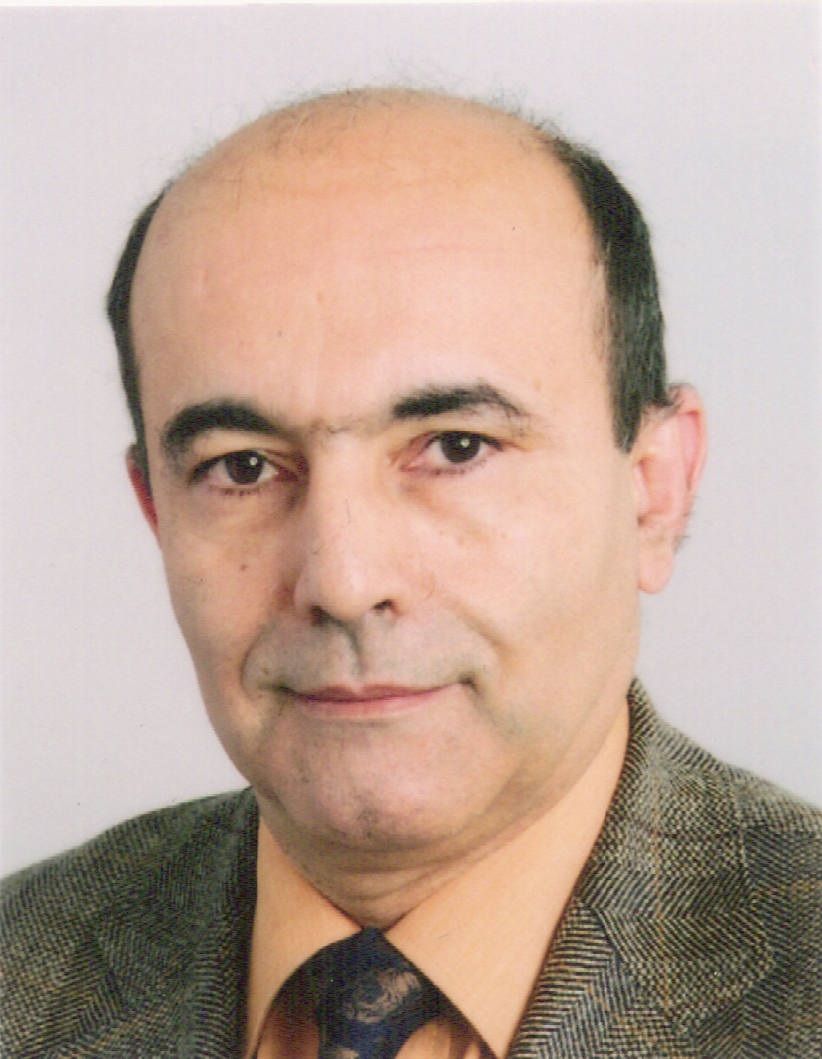
NAME: Ahmed Jerraya AFFILIATION: CEA-LETI COUNTRY: France BIO: Dr. Ahmed Jerraya is Director of Strategic Design Programs at CEA/LETI France. He served as General Chair for the Conference DATE in 2001, Co-founded MPSoC Forum (Multiprocessor system on chip) and served as the organization chair of ESWEEK2009. He supervised 51 PhD, co-authored 8 Books and published more than 250 papers in International Conferences and Journals TITLE: Convergence of Design and Fabrication Technologies, a Key Enabler for HW-SW Integration ABSTRACT: The last decade was dominated by HW-SW convergence where designers learned to combine hardware and software design to cope with the increased demand of lower cost and increased performances. This starting decade will be dominated by the convergence between design technology (HW and SW) and fabrication technologies. In fact more and more designs require a deep knowledge of technology characteristics to reach the required performances. On the other side, design technologies are more and more used to overcome fabrication process imperfection and to improve yield. This talk will first explain the achievements in HW-SW convergence and SoC design. Then, it will address the fabrication technology trends and challenges to deal with this convergence. Thursday, July 8th 8h20 - 9h10
NAME: Sani Nassif AFFILIATION: IBM Austin Research Laboratory COUNTRY: USA BIO: Sani Nassif received his PhD from Carnegie-Mellon University in 1986. He worked at Bell Labs until 1996 when he joined the IBM Austin Research Laboratory, where he currently manages the Silicon Analytics Department. Sani is an IEEE Fellow, member of IBM's Academy, and currently serves as the VP of Conferences for CEDA. TITLE: The Light at the end of the CMOS Tunnel ABSTRACT: ABSTRACT: In spite of numerous predictions to the contrary, Silicon technology is marching along past the 22nm node and on to ever-finer dimensions. Innovations at the technology, device, circuit and system levels continue to enable us to scale in spite of what sometime appear to be insurmountable problems in power, lack of performance, manufacturability and so on. To a large degree, these innovations are necessary because no substitute technology has been found as yet and, in fact, it does not appear likely that any such technology will become practical this decade. This leaves us with the need to anticipate and predict the near and medium term futures of CMOS for the next handful of technology nodes. This talk will focus on doing just that, and will show how an important new constraint on future system scaling is circuit resilience. Resilience is the ability of circuits to operate in spite of challenges like noise, difficult environmental conditions, ageing and manufacturing imperfections. These factors conspire to cause transient or permanent errors that are indistinguishable from traditional ”hard” faults typically caused by defects during fabrication. Without significant innovation at the circuit and system levels, the probability of these events can rise quite dramatically. In the area of SRAM, such phenomena have existed for the last three or four technology nodes, but significant investments in this area have indeed allowed continued system level scaling with ever-larger on-chip memories. As these same phenomena start attacking integrated circuits more pervasively, there is an urgent need for research and development in this area to avert the problems certain to arise with increased defect rates. This keynote paper explores the link between the old subject of manufacturing variability and its well known impact on circuit performance, and the new subject of the way that same variability -in the extreme- can cause complete circuit failure. With care, we will find that the light at the end of the CMOS tunnel is the opening of new opportunities to enrich CMOS with new technologies like MEMS, optics, sensors and even biological devices. Otherwise, that light is likely to be another train... |
|||||||||||||||||||||||||||||||
ASAP 2010 is organized by |
||||||||||||||||||||||||||||||||
|
Site last modified 2010-06-07


